


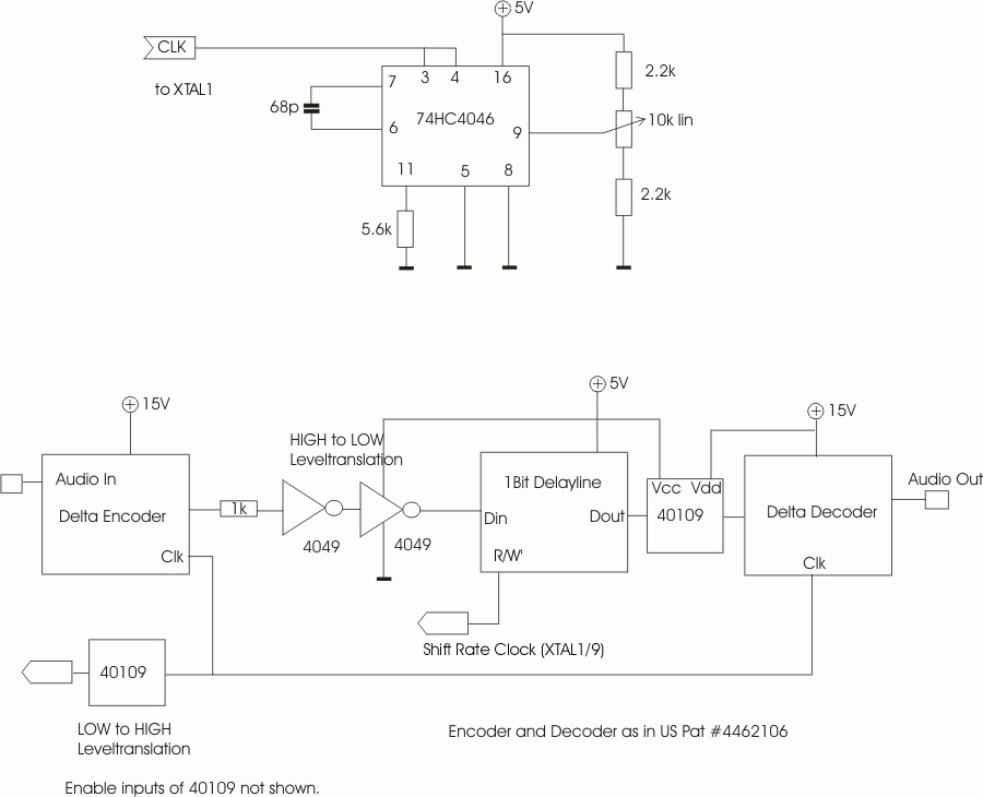
Simple 1-bit delayline
Introduction
This circuit started out with the need for a long shift register. I wanted to make a digital delayline, using the bit-serial encoders as described in the US-patent #4462106. The circuit shown is just the delay core, and is part of a larger system. In my opinion this is a good demonstration on how to interface a DRAM with an AVR microcontroller. To make it work with the delta encoders or similar ones, one needs to do some levelshifting.
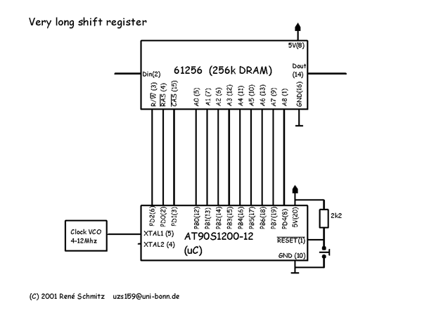
The circuit
Although one can make such a circuit from standard MSI parts, I opted for a uC based design. My choice fell on the AT90S1200 since they're pretty fast compared to a PIC. It lacks most of the fancy peripherals and the RAM that its bigger brothers (and sisters) have, but I didn't want to make use of them anyway. Anyway it should be straight forward to port it to another ATMEL device. The software is just a pretty short loop, that asserts the R/W' CAS' and RAS' lines in the proper order, and implements an 18-bit address counter that is multiplexed onto the 9 address lines of the DRAM. The 256k types where just what I have here in quantity, and if you have some old 286 or even 8088 based computer that you use as a door stopper, then you'll find plenty of them inside. I've also made a variant that uses 64k DRAMs. These will be connected only to the lines A0-A7. Also one could hack something out to use 1Mbit RAMs. The operation is quite simple, the input of the DRAM appears 256k R/W' cycles later at the output.
The way that the refresh is taken care of is worth a mention. Usually DRAMs were used with some kind of DRAM controller chip, the DRAM uses a cap for storing its information, and due to leakage they need to be periodically refreshed. You have to activate all rows in a given time, 8ms or so. But in this application we cycle through the adresses fast enough anyway we don't need to do an extra refresh cycle.
It's possible to extend the amount of RAM, by bussing the address lines and the R/W' CAS' and RAS' lines out to several DRAMs. You can either use them in parallel with some parallel ADC / DAC or chain them all in series for a bit serial encoder. In the latter case you simply tie the Din pin to the Dout of the preceeding DRAM.
To get hold of a clocking signal at the actual sampling rate (which is 1/9th of the uC clocking rate) you can make use of the R/W' line. I have had to shift that signal to send it to the encoders. (A level translator chip is handy here.) The clock for the uC is generated in a VCO of a 74HC4046 which can go up to 12MHz. I have the idea of makeing that into a PLL so that I can steer the delay time with trigger pulses, for easy interfacing with sequencers. When I get arround doing that I'll place the schematic here. Block level view of the entire delay.
The Firmware
What would a uC be without its software? Here are the files:
|
|
|
|
|
|
There might be some features to add, like setting the maximum delay time using a few switches, but I haven't got arround doing this. However if you make your own additions to the files here or find ways to improve the performance, you're free to publish it and please let me know.
Further ideas
I think there are many other uses for this circuit, like a trigger/pattern memory, if you feed the output back into the input via a resistor. To program you then supply your pulses with a low impedance to the input, and disconnect this lower impedance for the feedback to take over. It might also be interesting to interface a serial ADC/DAC to this circuit. Although the software would need modifications, and send some other control signals to the ADC/DAC. One then probably needs a refresh logic since one wouldn't need to clock the thing so high as I did. But the software could handle this.