


CMOS VCO
Introduction
The circuit presented here is aimed towards simplicity and ease of construction. It can be an addition to a modular system, used in a standalone fashion or as a test oscillator for your bench. I found it interesting to use the gates of a 4069 CMOS inverter instead of opamps. Sort of a VCO complement to the WASP filter elsewhere on this site.
Circuit overview
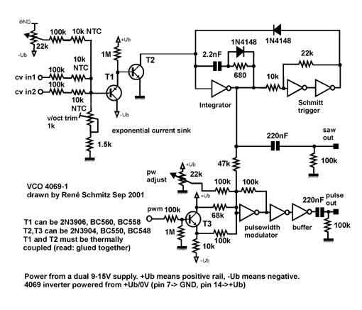
The circuit follows practically the same design pattern that most VCOs use. The input stage is summing up the presented control voltages. This stage is implemented here by a passive adder comprised out of the 100k summing resistors, the thermistors and the 1.5k in series with the 1k trimpot. The purpose of the latter is to set the VCO to 1Volts/octave. This summing stage usually follows an exponential current source. That is realized by the two transistors and the associated resistor. (Its called sink in the schematics because the current really flows into the output.) That current source (sink or whatever...) follows an integrator, that is converting the current into a rising voltage. The slope of the rise is proportional to the applied current. To make an oscillator one has to reset the rising slope to a lower voltage when it has reached a certain voltage, so that the output can rise again. That is the task of the two gates labelled schmitt trigger. A schmitt trigger is a circuit that sets when a high voltage is present, it fires. The circuit remains set until a much lower voltage is presented at the input. When the schmitt trigger is fired it discharges the integration capacitor thru the diode and the cycle can start again. At the output of the integrator there is a sawtooth waveform available. It is decoupled thru an RC combination which eliminates the DC offset from the signal.
The sawtooth signal is also fed into the part called pulsewidth modulator. The first gate is to sum up the control voltages for PWM with the signal which is then fed into the two series connected gates. The two gates combined have a high gain that shapes the pulse waveform out of the sawtooth. Another interesting very floppy pulse waveform is available at the output of the middle gate. I didn't draw a cap and resistor there, but the inclined builder might want to add that as well.
The circuit is having temperature compensation for the expo pair. The solution to that was to put 10k thermistors in series with the three 100k input summing resistors. The thermistors are cheap and easy to get, as they are NTCs, so the luxury of having three tempcos doesn't account much on the budget. If the room permits these should be coupled thermally to the transistors. Sometimes they are quite bulky. One could also interface a different expo source, for example the one of the VCO3 or 4. But the circuit would be a little more complex.
At 15V supply the 4069 gets a little hot. But not that hot that you would burn your finger. Two gates are biassed in "class A" mode, that means both transistors of the invertor are conducting simultaneously, so that the power dissipation is high.
Construction

The circuit can be easily constructed on a piece of pad per hole board. The picture shows how I constructed mine. The transistors are glued face to face, so that they have the same temperature. The transistors are the indicated BC5xx types. If you want to use the 2N390x types, watch out for the different pinout. These would need to be turned 180 degrees to fit into this layout. (Thanks for pointing this out go to Janne Heikkarainen.)
The black lines are connections that can either be made from short pieces of uninsulated wire (you'll have plenty of that after you cut the leads of the resistors), or for the connections between adjacent pads by making a bridge with solder. The purple lines are insulated wires which are connected directly to the pads on the solder side. These should be connected as the last, as it would be possible to melt the insulation when you have to work near them. The thick black spots denote where power enters the circuit and where the output waveforms can be obtained. If you're diverting from the layout here a warning is in order, as Scott Gravenhorst has discovered, the order of how the gates are used is somewhat critical, sometimes substititing one gate for another makes some parasitic oscillations, if you stick to the gate order here, there should be no problem, as well as with the one on Scotts site.
Also check out Scott Gravenhorsts site. He shows how to modify this circuit to accept a linear control voltage, and made some very cool waveshaper add-ons.
Scotts VCO with suboctave triangle

The circuit can detune if the load on the sawtooth output changes. Thanks for this discovery go out to Karl Ekdahl. To remedy this and to bring the amplitude up to the amplitude of the square output, this little circuit can be used.
Motohiko Takeda made a nice version of this oscillator, and a page dedicated to it. Be sure to check it out!
Sound example. (apologies to any JSB fans) Click here
Here is a partlist for this circuit.